PRINTING TECHNOLOGY
Addressing the challenges of flexible hybrid electronics with advanced printing
High Precision Capillary Printing (HPCaP) has been designed to deliver outstanding precision and resolution without relying on external forces, allowing it to adapt to diverse topographies and tackle significant challenges in flexible and hybrid electronics. Sahar al Kamand of Hummink explains the technology’s potential.
Research and development in flexible hybrid electronics (FHEs) are expanding rapidly due to their broad applications in various industries like healthcare and aerospace. Traditional lithography-based manufacturing processes are time-consuming, prompting a shift towards new direct-printing additive manufacturing techniques on both rigid and flexible substrates. The growing demand for flexible displays, wearable sensors and biomedical applications, particularly in point-of-care medicine, has highlighted the need for high-resolution printing techniques that work on various substrates. This demand has led to the development of new printing technologies, but many rely on external forces such as pressure or electric fields to expel ink, which limits versatility, precision and resolution, especially as printing dimensions shrink. High Precision Capillary Printing (HPCaP) has been developed to achieve exceptional precision and resolution without the need for external forces, making it adaptable to different topographies and addressing major challenges in flexible and hybrid electronics. High Precision Capillary Printing (HPCaP) is a technology inspired by Atomic
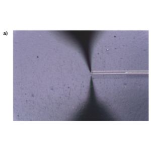
Figure 1a: Optical image of a glass pipette printing silver lines on a glass substrate.
Force Microscopy (AFM) that uses capillary forces and resonance as the sole driving mechanisms for printing. A macro resonator provides precise motion and feedback for printing. The resonance of the system can be finely tuned, allowing control over print characteristics such as thickness and line width. A pipette attached to the resonator dispenses ink by capillary action. The ink is drawn out by capillary forces allowing precise and consistent printing across different topographies. This advanced printing technology overcomes the challenges in flexible hybrid electronics through the following key features.
Micron and sub-micron resolution As electronic devices become smaller and more compact, the components within them such as circuits, transistors and sensors need to be miniaturised. Micron and sub-micron printing enables the precise manufacture of these tiny components. HPCaP offers high-resolution printing capabilities from 50 μm down to 100 nm, achieving precise output even at sub-micron level. It can print fine lines, such as the 2.5 μm wide silver lines on glass substrates in figure 1, which can be used as electrodes in
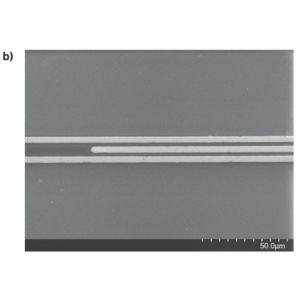
Figure 1b: SEM image of the same lines of 2,5 μm line width and 1,5 μm gap.
field-effect transistors. The technology also supports the printing of a variety of materials, including polymers and other inks, with high precision and adaptability to different substrate topographies. An example is the printing of polymer lines with a width of ca. 430 nm and a pitch of 1 μm to create sub-micron gratings for applications such as distributed feedback lasers (figure 2).
Adaptation to substrate topography The ability to print on various flexible substrates, such as polyimide and PET, is crucial for manufacturing flexible hybrid electronics (FHEs) and sensors, especially for applications requiring complex topographies like textiles. HPCaP technology excels in this area, automatically adapting to any substrate’s topography. For instance, it successfully printed durable silver pads on ultra-thin PET foil, which remained intact after multiple folds (figure 3). Additionally, HPCaP demonstrated precise printing on a wet-etched silicon wafer with a 100 μm step and a slope angle of 54.7°, maintaining continuous lines even at challenging edges (figure 4). The technology operates similarly to Atomic Force Microscopy (AFM), with advanced electronics that adjust the pipette‘s movement in real-time to match
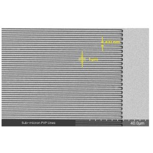
Figure 2: SEM image of printed Polyvinylpyrrolidone (PVP) lines (dark horizontal lines) at the sub-micron scale, with a gap of 1 micron (light gray horizontal lines).
THE AUTHOR Sahar al Kamand is a sales engineer at Hummink, where she is responsible for identifying new business opportunities and collaborating closely with the business development team to facilitate Hummink’s global expansion efforts. Her educational background includes a master’s degree in electronics engineering with a focus on biomedical applications, as well as a master’s degree in biomaterials and biodevices from the BME International Program in Paris. Sahar al Kamand has also gained experience in sales and business development within biomedical and technology companies, including start-ups.
THE COMPANY Hummink is a leading developer and supplier of High Precision Capillary Printing (HPCaP), an innovative technology revolutionising the display, semiconductor and printed electronics industries. Founded in 2020 by Amin M’barki (CEO) and Pascal Boncenne (COO), Hummink originated as a spinoff from Institut Pierre-Gilles de Gennes (IPGG), Ecole Normale Supérieure (ENS), CNRS and PSL University in Paris. In just three years, Hummink has successfully installed its printer “The NAZCA” across the USA, Europe and Asia, establishing a network of distributors and representatives worldwide. At present, Hummink is dedicated to expanding its global footprint and integrating its HPCaP technology into manufacturing workflows. www.hummink.com
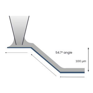
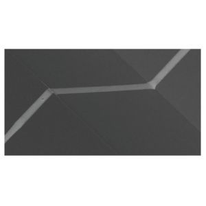
Figure 4: A SEM image of a silver trace printed on a wet-etched silicon wafer with a step of 100 μm and a slope of 54.7° angle (right) and the schematic representation.
the substrate‘s surface, enabling accurate printing without additional commands.
Diverse material compatibility The ability to print various inks on the same substrate is essential for flexible electronics. A significant challenge, particularly with textiles, is the need to print multiple materials using the same method, such as
alternating layers of conductive inks and polymers. HPCaP‘s use of capillary forces enables it to print inks with viscosities ranging from 0 to 100,000 cP. With only minor adjustments to the ink‘s rheological, capillary and colloidal properties, any ink can be used. In figure 5, we illustrate the capability to print 2 μm wide conductive silver lines on a silicon wafer and then coat these traces with a polymer (PVP), which is often necessary to prevent electrical shorts and oxidation of the metal.
Performance, functionality, flexibility Unlike the costly and error-prone multi-step process of cleanroom-based microfabrication, printing methods offer notable advantages in terms of cost-effectiveness and reliability. High Precision Capillary Printing (HPCaP) is a technique with significant applications in flexible hybrid electronics. HPCaP‘s ability to print micron and sub-micron structures, adapt to various substrate topographies and work with a wide range of materials underscores its potential to overcome the challenges in flexible hybrid electronics and thus play a crucial role in advancing the development and production of the next generation electronic devices with enhanced performance, functionality and flexibility.
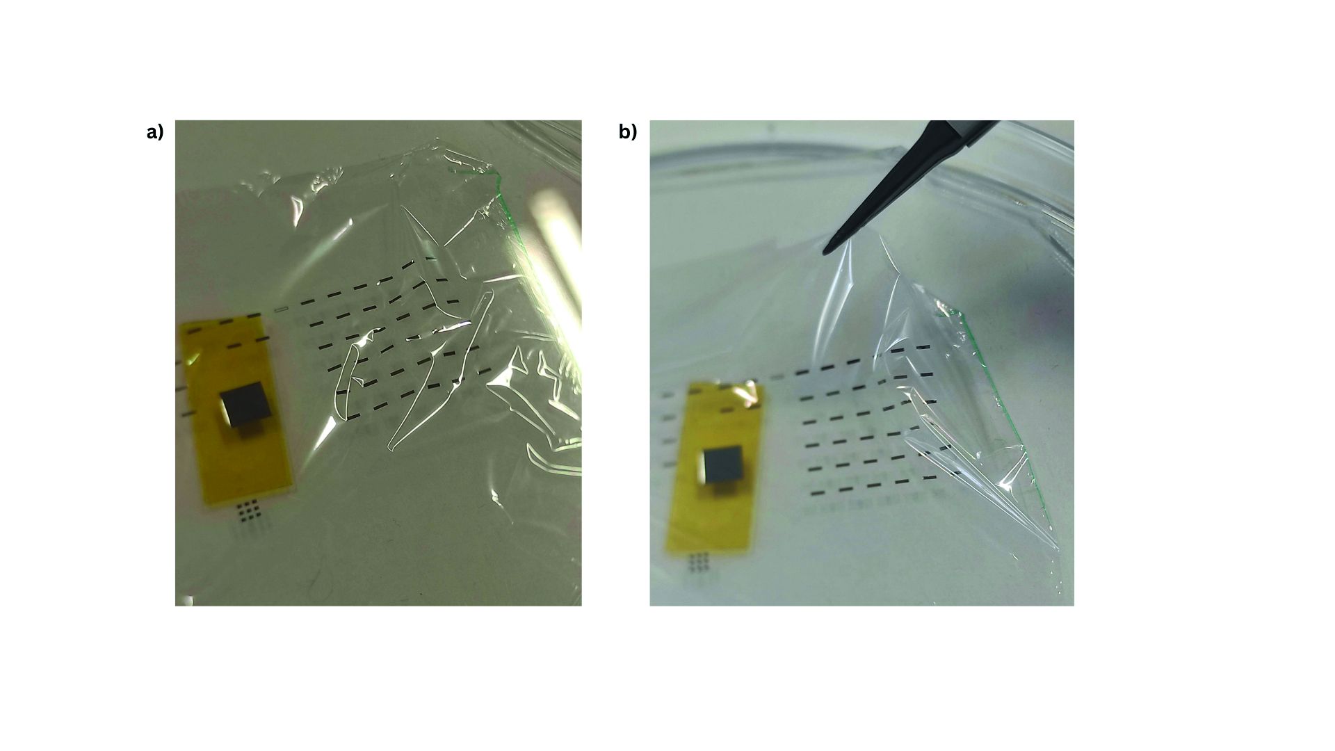
Figure 3a: Rectangle silver pads printed on PET foil of 3 μm thickness. Figure 3b: Image of the printed silver pads showing their flexible performance.
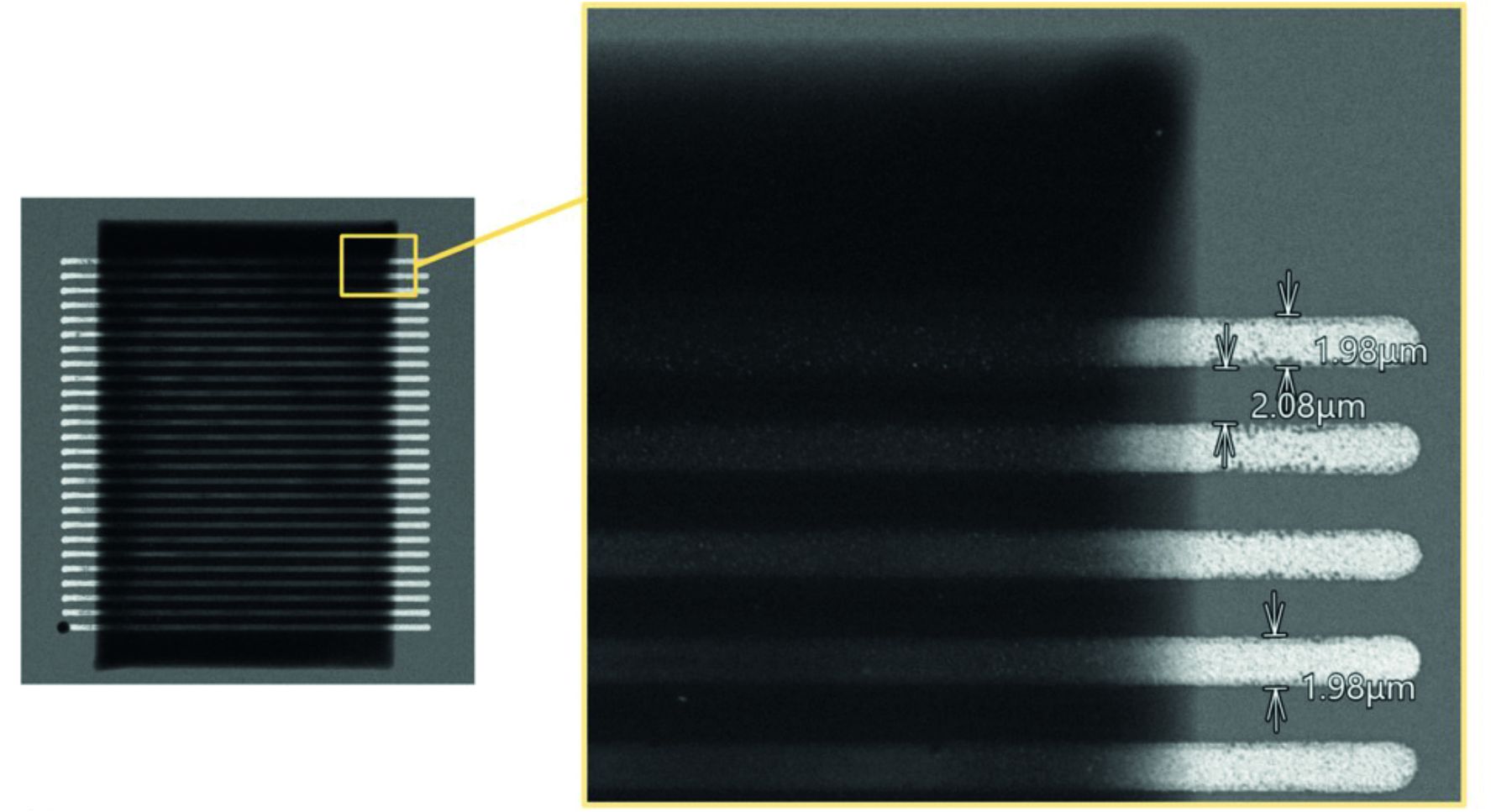
Figure 5: SEM Image of printed silver lines of 2 μm linewidth and 2 μm pitch on silicon wafer coated by HPCaP as well with traces of PVP.