MATERIALS AND COMPONENTS
Smart Printing for Sustainable Manufacturing
The contemporary electronics manufacturing landscape emphasizes sustainability due to technological advancements and demand for electronic products. This growth in production has raised concerns about electronic waste. Printed electronics emerges as a pivotal solution, leveraging its capacity for lower material usage through additive printing. Sahar al Kamand of Hummink (France) explains how the company’s High Precision Capillary Printing (HPCAP) technology aligns with eco-friendly objectives.
IDTechEx's recently released report, “Sus-tainable Electronics Manufacturing: 2023-2033,” discusses minimizing the environmen-tal footprint associated with the production of printed circuit boards (PCBs) and integrated circuits (ICs). The report explores the potential of innovative processing methods and judi-cious materials selection in mitigating the environmental impact of these manufactur-ing processes. This involves the adoption of low-temperature processing, the elimination of redundant and wasteful steps, the promo-tion of recycling and reusing materials when-ever feasible, and the incorporation of novel approaches with long-term sustainability potential.
Among the solutions presented in the report, High Precision Capillary Printing (HPCAP) technology stands out as a key ena-bler across these recommended strategies. In the following sections, we explain how HPCAP technology aligns seamlessly with the suggested sustainable solutions.
Capillary Forces are the Only Driving Force
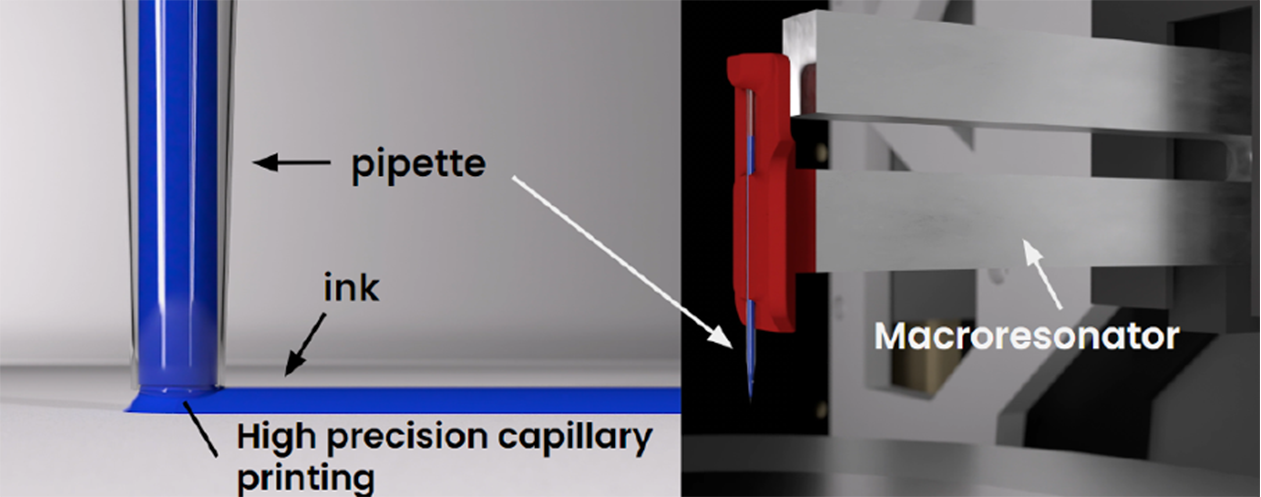
HPCAP technology relies exclusively on capillary forces; they are the only driving force to enable printing on different substrates. Drawing inspiration from Atomic Force Microscopy (AFM), HPCAP employs a macro-resonator as its primary sensing mechanism to provide feedback during contact and print-ing processes. As it is clear in Figure 1, the macro-resonator oscillates at a resonance frequency of about 1 kHz and is attached to a mechanical bridge. State-of-the-art elec-tronics are used to control the resonance of the macro-resonator through three different parameters: the resonance phase, amplitude, and frequency. Any shift in these values can be controlled to achieve different printing fea-tures, indirectly modifying the print geometry (e.g. thickness, line width). Amplitude can be adjusted between 5 nm and 100 nm, and any frequency shift of 100 mHz or more can be accurately detected.

Figure 1. Illustration of the macro-resonator and the pipette attached.
A glass pipette is attached to the extremi-ty of the macro-resonator and oscillates in phase with the latter. This pipette is made of a pulled glass capillary; and despite its fragility, the real-time detection of interac-tion between the substrate and the pipette avoids any uncontrolled damage to both the substrate and the pipette, while maintain-ing a high-quality dispensing mechanism. By controlling the pulling parameters (e.g. heat, force), a wide range of pipette diameter can be achieved, from 100 nm to 50 μm.
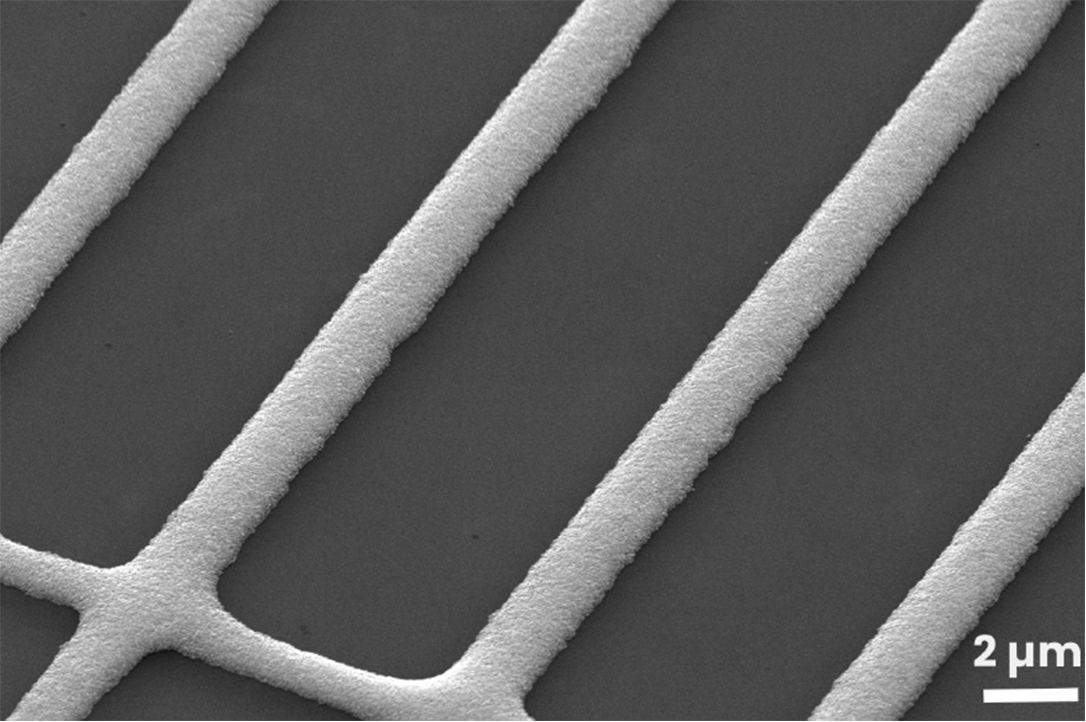
HPCAP guarantees the precise and unin-terrupted printing of any ink, as evidenced in Figure 2, showcasing silver lines with a nota-ble absence of splashes or satellite drop. This advantage is attributed to capillary forces, wherein the absence of applied pressure ensures the complete utilization of all materi-als within the pipette, resulting in a zero-waste printing process. Additionally, the technology allows the pipette to be filled with various inks, typically in small quantities measured in tens of microliters. Leveraging dispensed vol-umes in the nanoliter range (orders of magni-tude lower than the pipette's total volume), a single pipette possesses the capacity to print distances of up to hundreds of kilometers, depending on the dispensing diameter. This remarkable efficiency implies that even very small volumes of ink are sufficient to produce an extensive array of samples.

Figure 2. Micron scale silver lines.
A Complementary Solution with Photolithography
Photolithography stands out as the highest-resolution patterning technique widely employed in the semiconductor indus-try. However, it involves numerous steps, demanding a significant amount of resources and money. Printing technologies face chal-lenges as direct substitutes for photolitho-graphy, mainly due to resolution limitations. On the other hand, HPCAP emerges as a promising complementary solution, reducing the number of steps and boasting resolutions up to 100 nm. Given that HPCAP can replace some steps done by lithography, it operates as an additive manufacturing technology that directly prints onto the substrate.
A comprehensive comparison between photolithography and HPCAP is presented in Table 1. HPCAP excels by reducing the num-ber of steps, exhibiting significantly faster processing times, being more cost-effective and minimizing material waste to nearly zero. This comprehensive analysis underscores the advantages of HPCAP, emphasizing on its eco-friendly attributes and positioning it as a compelling complementary solution for high-resolution and resource-efficient patterning in electronic manufacturing.
An example of the importance of HPCAP in reducing the effort needed, i.e additive manufacturing components, is the All-printed SU8-perovskite DFB laser. In a publication, the authors demonstrate the fabrication of a Distributed Feedback (DFB) laser from addi-tive manufacturing techniques only. This laser is composed of SU8 as the grating and of a perovskite thin film as the active medium. The SU8 grating is directly printed on glass with a pitch of 370 nm thanks to Hummink’s HPCAP technology, while the perovskite is simply spin-coated on top of the SU8. Their approach proves to be a fast and versatile tool for the fabrication and design of DFB lasers and wave-guides in general.
Table 1. HPCAP benefits compared to lithography.
HPCAP for Repair and Remanufacturing
Repair plays a crucial role in promot-ing sustainability across various industries. For instance, repairing and remanufacturing electronic devices, displays, semiconductors and automotive components allows for the preservation and reuse of valuable materials. By keeping products in use for longer periods, repair also contributes to reducing the environmental impact associated with waste generation and disposal. Moreover, repairing products contribute to reducing the need for continuous manufacturing, consequently lowering overall emissions associated with production.
HPCAP technology contributes to the repair process in several industries including display, electronics, semiconductor and automotive. In the case of display repair, the indus-try is looking for technical solutions able to repair new generations of thin film transistors (TFT) and color converters with high precision at micron scale. Conventional methods are failing at this scale.
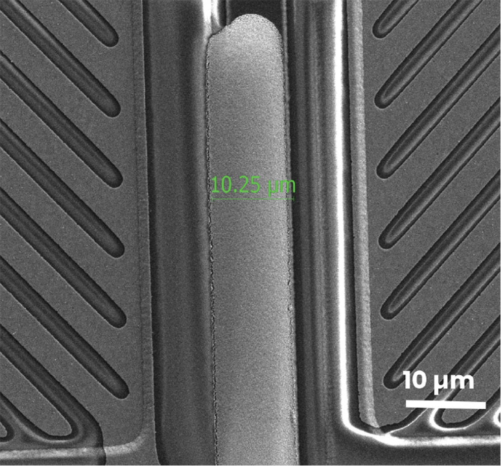
HPCAP technology is a perfect solution thanks to its high precision, as it fully removes satellite drops and particles generated by conventional technologies. Figure 3 shows TFT repair lines printed by HPCAP.

Figure 3. TFT repair lines by HPCAP.

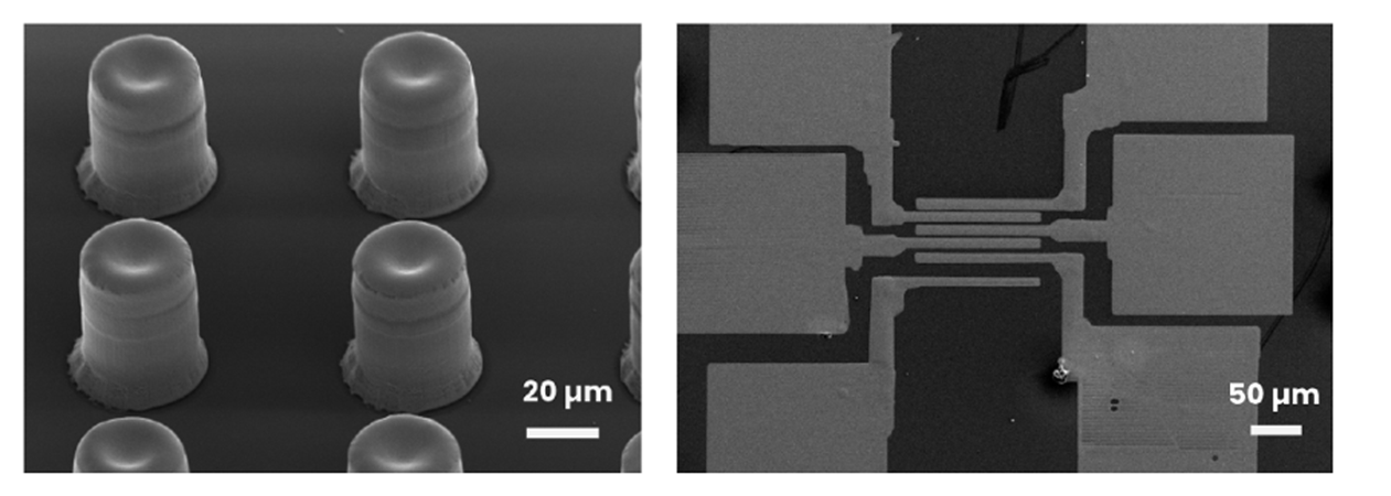
Figure 4. Bumps and pads printed by HPCAP.
Repair has even reached the semicon-ductor industry; as fan-out manufacturing is transitioning from wafers to panels, the cost of each panel becomes very significant, and the industry is looking for technical solutions able to repair metallization defects at the micron-scale. Again, conventional methods, such as inkjet and CVD repair, cannot repair at such a high resolution, while HPCAP meets the requirements of RDL (redistribution layer), bumps and pads open defects repair, at the micron-scale and beyond. In addition to the absence of any satellite drops that improve the repair yield. Figure 4 shows bumps and pads printed by HPCAP.
Repair is the current trend in the automo-tive industry including the remanufacturing and repair of several automotive components. An interesting article by Guillaume Guichard discussed repair in detail and mentioned the need of micron and sub-micron resolutions in some components (Guichard, 2024). That is again where HPCAP can come in handy and again contribute in sustainability and smart manufacturing.
In the pursuit of sustainability and smart printing technologies HPCAP stands out. In the dynamic landscape of electronics production, where demand surges and environmental concerns escalate, HPCAP emerges as a solu-tion that not only minimizes material usage through additive printing, but also actively promotes sustainability. The comparison with traditional methodologies, such as photo-lithography, highlights HPCAP's efficiency, cost-effectiveness and minimal waste genera-tion. Beyond manufacturing, HPCAP's appli-cation in repair industries, from electronics to semiconductors and automotive components, showcases its versatility and high precision at the micron and sub-micron scales. As we journey towards a circular economy and eco-conscious innovation, additive manufacturing technologies like HPCAP pave the way for a more resilient, efficient and environmentally friendly future.
Author: Sahar al Kamand

Sahar al Kamand
Sahar al Kamand is a sales engineer at Hummink, where she is responsible for identifying new business opportunities and collaborating closely with the busi-ness development team to facilitate Hummink's global expansion efforts. Her educational background includes a master’s degree in electronics engineering with a focus on biomedical applications, as well as a master's degree in biomaterials and biodevices from the BME Interna-tional Program in Paris. Sahar al Kamand has also gained experience in sales and business development within biomedical and technology companies, including start-ups.
Hummink
Hummink is a leading developer and sup-plier of High Precision Capillary Printing (HPCAP), an innovative technology revo-lutionizing the display, semiconductor and printed electronics industries. Founded in 2020 by Amin M'barki (CEO) and Pascal Boncenne (COO), Hummink originated as a spinoff from Institut Pierre-Gilles de Gennes (IPGG), Ecole Normale Supérieure (ENS), CNRS and PSL University in Paris. In just three years, Hummink has successfully installed its printer "The NAZCA" across the USA, Europe and Asia, establishing a network of distributors and representa-tives worldwide. At present, Hummink is dedicated to expanding its global footprint and integrating its HPCAP tech-nology into manufacturing workflows.
