NEWS
Fraunhofer FEP: Innovative roll-to-roll plasma process for graphene layers
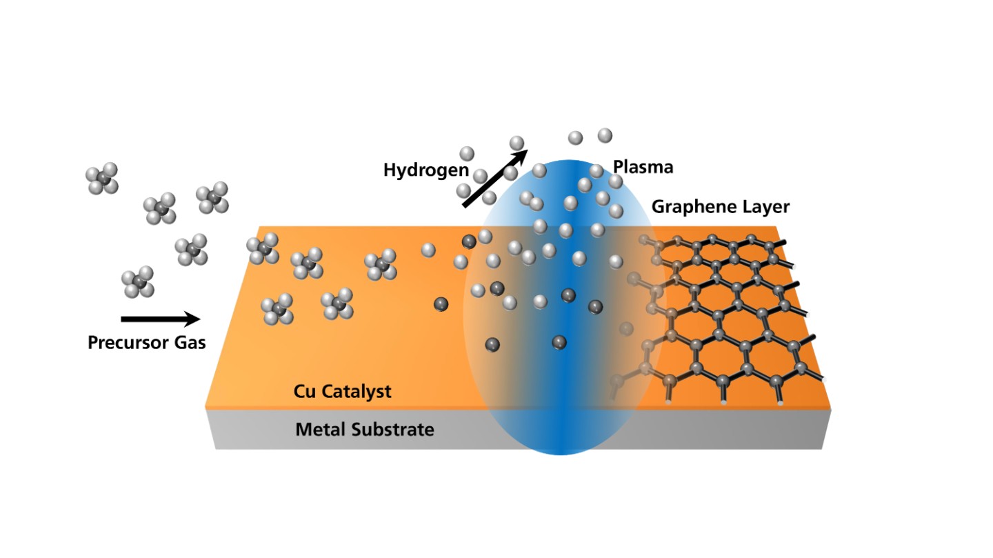
Scheme of the PECVD synthesis process for graphene. Image source: Fraunhofer FEP
Graphene layers promise great progress and increased efficiency in solar applications, energy storage and smart glass applications due to their outstanding properties, including transparency, barrier effect and conductivity. The lack of scalable deposition processes with consistently high layer quality at cost-efficient throughputs has so far prevented the breakthrough of this material.
As part of the funded EU project NewSkin, the Fraunhofer Institute for Electron Beam and Plasma Technology FEP from Dresden, Germany, has developed an innovative PECVD process that enables the deposition of graphene at high process speeds and offers higher production throughputs and a wider range of substrates at lower process temperatures.
The researchers at Fraunhofer FEP took advantage of the versatility of the inline coating tool MAXI. Depending on the maturity of the process, the multifunctional vacuum coating plant offers the possibility to run processes in sheet-to-sheet as well as in roll-to-roll mode. Moreover, the variety of processes at the MAXI allows for pilot production, providing good prerequisites for the development and scaling of graphene deposition processes.
Dr Stefan Saager, group leader for coating metal and energy technology, explains: “Graphene can be deposited on metallic strips using the innovative PECVD process in the roll-to-roll mode. In the first step, the metal strip is coated with a thin layer of a catalyst material such as copper in vacuum. This allows the desired substrate material to be selected independently of the suitable catalyst material. The coated metal strip is then fed into a process unit containing an argon plasma. Its argon ions collide with the substrate and heat it in a very short time. By adding suitable precursor gases such as methane or acetylene, the respective molecules can be cracked into their constituents and partially ionised at the same time. Ideally, the resulting carbon atoms and ions are deposited on the substrate in a monolayer, well-ordered 2D structure, thus synthesising the desired layer of graphene.”
In the next step, the scientists at Fraunhofer FEP are going to work on the reproducibility of the results and on the further improvement of the layer properties, e. g. the number of graphene layers.
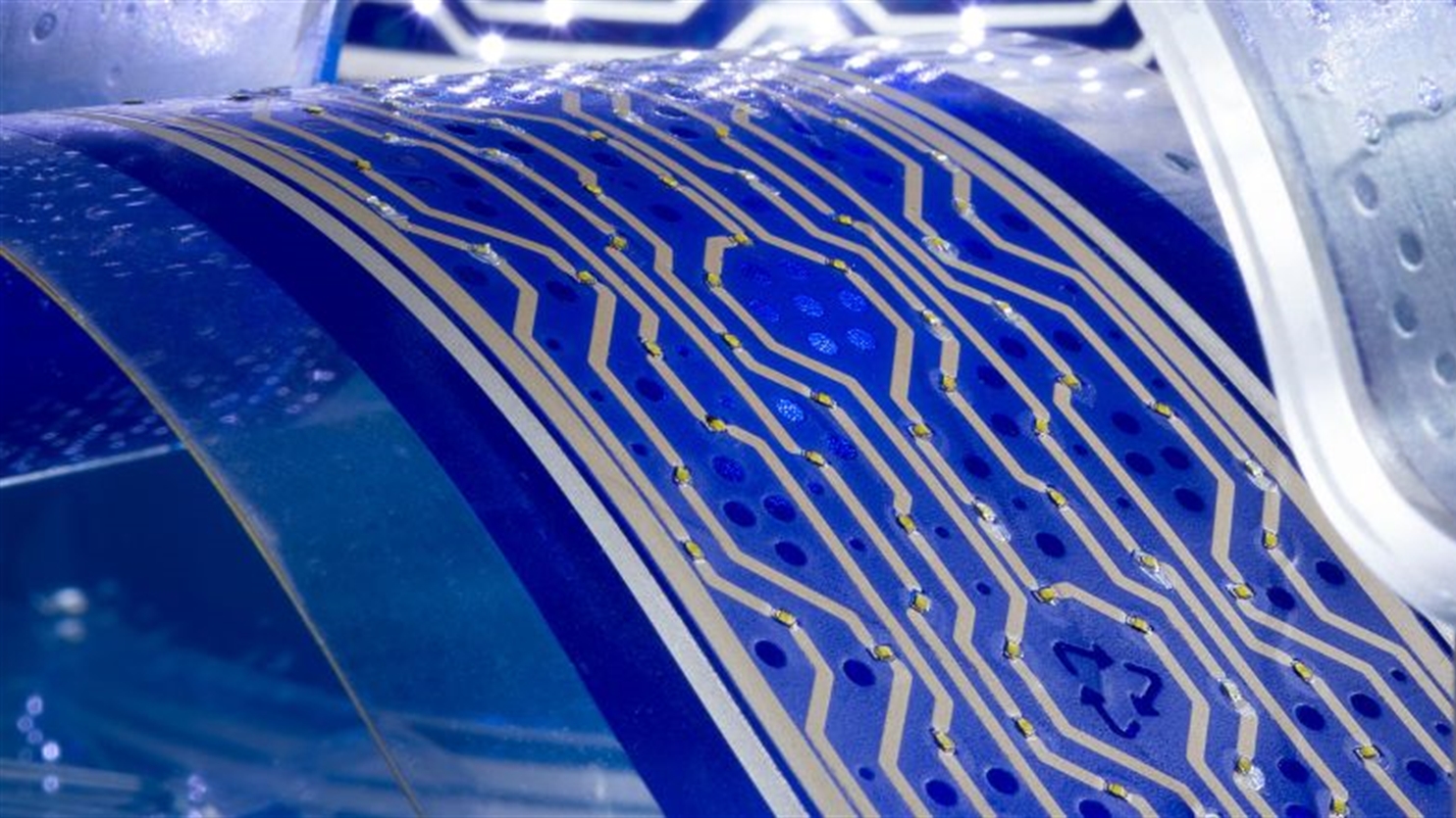
TNO develops first method for fully circular electronics
TNO at Holst Centre, Eindhoven, the Netherlands, has developed a new disassembly method that allows electronics to be removed from the carrier at the end of the product‘s life, enabling recycling and repair. Companies are increasingly using printed forms of electronics because they can be seamlessly integrated into almost any product. To protect the electrical circuitry, the electronic components and printed metals are fused with plastics. This makes repair and recycling virtually impossible. Only a fifth of all electronic waste worldwide is currently properly recycled. The amount of electronic waste is estimated to reach 74.7 million tons by 2030 and 110 million tons by 2050.
To disassemble this printed form of electronics, TNO has developed a special water-based layer. It was applied between the circuit with components and the outer plastic layer of the electronic test device. Tests showed that the layer was strong enough to withstand 1000 hours of up to 85% humidity and a temperature of 85°C. At the same time, the new layer is flexible enough to allow the plastic to be removed without damaging the electronic circuitry.